日志
[ZZ]BiCMOS Technology: Fabrication and Applications
| ||
At present, in every electrical and electronic device which we use in our daily life consists of integrated circuits which are manufactured by utilizing the semiconductor device fabrication process. The electronic circuits are created on a wafer made up of pure semiconductor materials such as silicon and other semiconductor compounds with multiple steps involving photo lithography and chemical processes.
The process of semiconductor manufacturing was started from Texas in early 1960’s and then extended all over the world.
BiCMOS Technology
This is one of the major semiconductor technologies and is a highly developed technology, in 1990’s incorporating two separate technologies, namely bipolar junction transistor and CMOS transistor in a single modern integrated circuit. So, for the better indulgent of this technology, we can have glance at CMOS technology and Bipolar technology in brief.
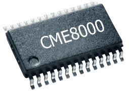
The figure shown is the first analog/digital receiver IC and is a BiCMOS integrated receiver with very high sensitivity.
CMOS Technology
It is a complementary of MOS technology or CSG (Commodore Semiconductor Group) which was started as source for manufacturing the electronic calculators. After that complementary of MOS technology called CMOS technology is used for developing the integrated circuits such as digital logic circuits along with microcontrollers and microprocessors. CMOS technology affords benefit of less power dissipation and low noise margin with high packing density.
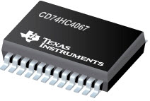
The figure shows the utilization of CMOS technology in manufacturing the digital controlled switch devices.
Bipolar Technology
Bipolar transistors are part of integrated circuits and their operation is based on two types of semiconductor material or depends on both types of charge carriers holes and electrons.These are generally classified into two types as PNP and NPN,classified based on doping of its three terminals and their polarities. It affords high switching as well as input/output speed with good noise performance.
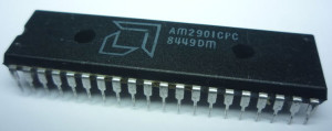
The figure shows the utilization of bipolar technology in RISC processor AM2901CPC.
BiCMOS Logic
It is a complex processing technology that provides NMOS and PMOS technologies amalgamated each other with the advantages of having very low power consumption bipolar technology and high speed over CMOS technology.MOSFETs grant high input impedance logic gates and bipolar transistors provide high current gain.
14 Steps for BiCMOS Fabrication
The BiCMOS fabrication combines the process of fabrication of BJT and CMOS, but merely variation is a realization of the base.The following steps show the BiCMOS fabrication process.
Step1: P-Substrate is taken as shown in the below figure

Step2: The p-substrate is covered with the oxide layer

Step3: A small opening is made on the oxide layer

Step4: N-type impurities are heavily doped through the opening

Step5: The P – Epitaxy layer is grown on the entire surface

Step6: Again, entire layer is covered with the oxide layer and two openings are made through this oxide layer.

Step7: From the openings made through oxide layer n-type impurities are diffused to form. n-wells

Step8: Three openings are made through the oxide layer to form. three active devices.
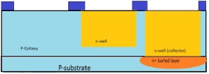
Step9: The gate terminals of NMOS and PMOS are formed by covering and patterning the entire surface with Thinox and Polysilicon.
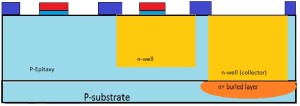
Step10: The P-impurities are added to form. the base terminal of BJT and similar, N-type impurities are heavily doped to form. emitter terminal of BJT, source and drain of NMOS and for contact purpose N-type impurities are doped into the N-well collector.
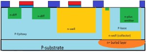
Step11: To form. source and drain regions of PMOS and to make contact in P-base region the P-type impurities are heavily doped.
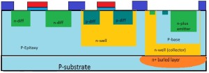
Step12: Then the entire surface is covered with the thick oxide layer.
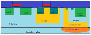
Step13: Through the thick oxide layer the cuts are patterned to form. the metal contacts.
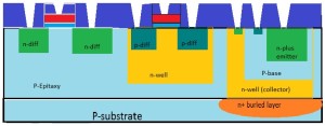
Step14: The metal contacts are made through the cuts made on oxide layer and the terminals are named as shown in the below figure.
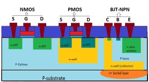
The fabrication of BICMOS is shown in the above figure with a combination of NMOS, PMOS and BJT. In the fabrication process some layers are used such as channel stop implant, thick layer oxidation and guard rings.
The fabrication will be theoretically difficult for including both the technologies CMOS and bipolar. Parasitical bipolar transistors are produced inadvertently is a problem of fabrication while processing p-well and n-well CMOS. For the fabrication of BiCMOS many additional steps added for fine tuning of bipolar and CMOS components. Hence, the cost of total fabrication increases.
Channel stopper is implanted in semiconductor devices as shown in the above figureby using implantation or diffusion or other methods in order to limit the spreading of channel area or to avoid the formation of parasitic channels.
The high impedance nodes if any, may cause the surface leakage currents and to avoid the flow of current in places where the current flow is restricted these guard rings are used.
Advantages of BiCMOS technology
- analog amplifier design is facilitated and improved by using high impedance CMOS circuit as input and remaining are realized by using bipolar transistors.
- BiCMOS is essentially vigorous to temperature and process variations offering good economical considerations (high percentage of prime units) with less variability in electrical parameters.
- High load current sinking and sourcing can be provided by BiCMOS devices as per requirement.
- Since it is a grouping of bipolar and CMOS technologies we can use BJT if speed is a critical parameter and we can use MOS if power is a critical parameter and it can drive high capacitance loads with reduced cycle time.
- It has low power dissipation than bipolar technology alone.
- This technology found frequent applications in Analog power managing circuits and amplifier circuits such as BiCMOS amplifier.
- It is well appropriate for input/ouput intensive applications, offers flexible inputs/outputs (TTL, CMOS and ECL).
- It has the advantage of improved speed performance compared to CMOS technology alone.
- Latch up invulnerability.
- It has the bidirectional capability (source and drain can be interchanged as per requirement).
Drawbacks of BiCMOS technology
- The fabrication process of this technology is comprised of both the CMOS and bipolar technologies increasing the complexity.
- Due to increase in the complexity of the fabrication process, the cost of fabrication also increases.
- As there are more devices, hence, less lithography.
BiCMOS technology and Applications
- It can be analyzed as AND function of high density and speed.
- This technology is used as an alternate of the previous bipolar, ECL and CMOS in the market.
- In some applications (in which there is finite budget for power) the BiCMOS speed performance is better than the that of bipolar.
- This technology is well suited for the intensive input/output applications.
- The applications of BiCMOS were initially in RISC microprocessors rather than traditional CISC microprocessors.
- This technology excels its applications, mainly in two areas of microprocessors such as memory and input/output.
- It has a number of applications in analog and digital systems, resulting in the single chip spanning the analog-digital boundary.
- It overpass the gap permitting course of action and circuit margins to be crossed.
- It can be used for sample and hold applications as it provides high impedance inputs.
- This is also used in applications such as adders, mixers, ADC and DAC.
- To conquer the limitations of bipolar and CMOS operational amplifiers the BiCMOS processes are used in designing the operational amplifiers. In Operational amplifiers, high gain and high frequency characteristics are desired. All these desired characteristics can be gained by using these BiCMOS amplifiers.
The BiCMOS technology along with its fabrication, advantages, disadvantages and applications are discussed in brief in this article. For better understanding about this technology, please post your queries as your comments below.
Photo Credits:
- BiCMOS CME8000 by c-max-time
- CMOS CD74HC4067 by bdtic
- Bipolar AM2901CPC by silirium

 /1
/1 


 eetop公众号
 创芯大讲堂
创芯大讲堂 创芯人才网
创芯人才网