日志
Vivado下创建基于AXI-Lite的用户IP核(转)
| |
本文是为一位网友所写,据说网上Vivado下自定义IP核的资料很难找~本文主要讲述了在Vivado下创建AXI-Lite型IP核的流程。最近问IP问题的人略多……
Vivado为设计人员提供了很多IP核,但不可能完全满足我们的所有设计需求,在设计过程中,很多时候需要设计个性化的IP核,用于完成自己想要的功能。因此,在Vivado下创建IP核的流程也是必须掌握的基础之一。
废话不多说,直奔主题。
如图1所示,Tools > Create and Package IP…,打开IP创建和打包向导。

图1
进入第一个界面,如图2所示。是一些提示信息,直接点击Next
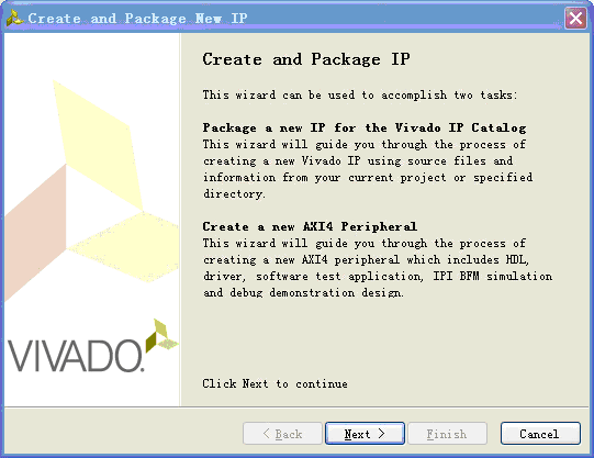
图2
进入操作类型选择界面,如图3所示。

图3
这里我们要做的是创建IP,所以选择“Create a new AXI4 peripheral”,如图3所示,选择完毕,单击next,进入下一界面,如图4所示。

图4
在该界面设置IP核的名称、版本、存储路径等,完毕后,点击Next,进入下一界面,如图5所示。

图5
此处可以设置总线类型、总线位宽、寄存器个数等,我们要做的就是一个AXI-Lite型IP,所以不必改动,直接Next,进入最后一步,如图6所示。

图6
向导的最后一步,IP概要信息,选择下一步操作。这里我们选择“Add IP to therepository”,这样在IP Catalog中就可以找到我们新建的IP了。
打开IP Catalog,在搜索框内键入myip(你的Ip的名字),就可以检索出IP核,如图7所示。

图7
选中该IP,右键,在弹出菜单中选择Edit in IP Packager,如图8所示。
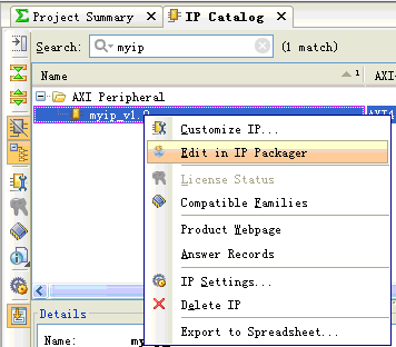
图8
之后会弹出对话框,询问新的工程存放路径及工程名称,如图9所示。
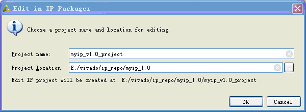
图9
设置完毕后,点击OK,会新建一个vivado工程,用于编辑IP核。
在新打开的Vivado IDE中,找到Source子窗口,双击打开myip_v1_0.v顶层文件(图10所示位置),在图11所示的位置添加自主端口,我这里是一个1bit的pwm_out输出端口。

图10

图11
所添加的pwm_out端口是连接到底层端口的,因此,需要添加相应的例化语句。在myip_v1_0.v中如图12所示位置添加例化语句,修改完毕后保存。

图12
顶层修改完了,再修改底层的module,具体修改部位就不说了,直接把修改后的代码贴出来,这里不是重点,感兴趣的话自己看一下吧。想设计PWM IP核,可以参考我之前的文章,用HLS做,比本文的方法简单快捷。
`timescale 1 ns / 1 ps

	module myip_v1_0_S00_AXI #
	(
		// Users to add parameters here

		// User parameters ends
		// Do not modify the parameters beyond this line

		// Width of S_AXI data bus
		parameter integer C_S_AXI_DATA_WIDTH	= 32,
		// Width of S_AXI address bus
		parameter integer C_S_AXI_ADDR_WIDTH	= 4
	)
	(
		// Users to add ports here
        output wire pwm_out,
		// User ports ends
		// Do not modify the ports beyond this line

		// Global Clock Signal
		input wire  S_AXI_ACLK,
		// Global Reset Signal. This Signal is Active LOW
		input wire  S_AXI_ARESETN,
		// Write address (issued by master, acceped by Slave)
		input wire [C_S_AXI_ADDR_WIDTH-1 : 0] S_AXI_AWADDR,
		// Write channel Protection type. This signal indicates the
    		// privilege and security level of the transaction, and whether
    		// the transaction is a data access or an instruction access.
		input wire [2 : 0] S_AXI_AWPROT,
		// Write address valid. This signal indicates that the master signaling
    		// valid write address and control information.
		input wire  S_AXI_AWVALID,
		// Write address ready. This signal indicates that the slave is ready
    		// to accept an address and associated control signals.
		output wire  S_AXI_AWREADY,
		// Write data (issued by master, acceped by Slave)
		input wire [C_S_AXI_DATA_WIDTH-1 : 0] S_AXI_WDATA,
		// Write strobes. This signal indicates which byte lanes hold
    		// valid data. There is one write strobe bit for each eight
    		// bits of the write data bus.
		input wire [(C_S_AXI_DATA_WIDTH/8)-1 : 0] S_AXI_WSTRB,
		// Write valid. This signal indicates that valid write
    		// data and strobes are available.
		input wire  S_AXI_WVALID,
		// Write ready. This signal indicates that the slave
    		// can accept the write data.
		output wire  S_AXI_WREADY,
		// Write response. This signal indicates the status
    		// of the write transaction.
		output wire [1 : 0] S_AXI_BRESP,
		// Write response valid. This signal indicates that the channel
    		// is signaling a valid write response.
		output wire  S_AXI_BVALID,
		// Response ready. This signal indicates that the master
    		// can accept a write response.
		input wire  S_AXI_BREADY,
		// Read address (issued by master, acceped by Slave)
		input wire [C_S_AXI_ADDR_WIDTH-1 : 0] S_AXI_ARADDR,
		// Protection type. This signal indicates the privilege
    		// and security level of the transaction, and whether the
    		// transaction is a data access or an instruction access.
		input wire [2 : 0] S_AXI_ARPROT,
		// Read address valid. This signal indicates that the channel
    		// is signaling valid read address and control information.
		input wire  S_AXI_ARVALID,
		// Read address ready. This signal indicates that the slave is
    		// ready to accept an address and associated control signals.
		output wire  S_AXI_ARREADY,
		// Read data (issued by slave)
		output wire [C_S_AXI_DATA_WIDTH-1 : 0] S_AXI_RDATA,
		// Read response. This signal indicates the status of the
    		// read transfer.
		output wire [1 : 0] S_AXI_RRESP,
		// Read valid. This signal indicates that the channel is
    		// signaling the required read data.
		output wire  S_AXI_RVALID,
		// Read ready. This signal indicates that the master can
    		// accept the read data and response information.
		input wire  S_AXI_RREADY
	);

	// AXI4LITE signals
	reg [C_S_AXI_ADDR_WIDTH-1 : 0] 	axi_awaddr;
	reg  	axi_awready;
	reg  	axi_wready;
	reg [1 : 0] 	axi_bresp;
	reg  	axi_bvalid;
	reg [C_S_AXI_ADDR_WIDTH-1 : 0] 	axi_araddr;
	reg  	axi_arready;
	reg [C_S_AXI_DATA_WIDTH-1 : 0] 	axi_rdata;
	reg [1 : 0] 	axi_rresp;
	reg  	axi_rvalid;

    //------------------ add by cuter---------------
    wire                                ovpprd;
    wire                                pwm_out_tmp;
    reg     [C_S_AXI_DATA_WIDTH-1:0]    pwm_cnt;
    //-----------------------end--------------------
	// Example-specific design signals
	// local parameter for addressing 32 bit / 64 bit C_S_AXI_DATA_WIDTH
	// ADDR_LSB is used for addressing 32/64 bit registers/memories
	// ADDR_LSB = 2 for 32 bits (n downto 2)
	// ADDR_LSB = 3 for 64 bits (n downto 3)
	localparam integer ADDR_LSB = (C_S_AXI_DATA_WIDTH/32) + 1;
	localparam integer OPT_MEM_ADDR_BITS = 1;
	//----------------------------------------------
	//-- Signals for user logic register space example
	//------------------------------------------------
	//-- Number of Slave Registers 4
	reg [C_S_AXI_DATA_WIDTH-1:0]	slv_reg0;             // used as period register
	reg [C_S_AXI_DATA_WIDTH-1:0]	slv_reg1;             // used as duty register
	reg [C_S_AXI_DATA_WIDTH-1:0]	slv_reg2;
	reg [C_S_AXI_DATA_WIDTH-1:0]	slv_reg3;
	wire	 slv_reg_rden;
	wire	 slv_reg_wren;
	reg [C_S_AXI_DATA_WIDTH-1:0]	 reg_data_out;
	integer	 byte_index;

	// I/O Connections assignments

	assign S_AXI_AWREADY	= axi_awready;
	assign S_AXI_WREADY	= axi_wready;
	assign S_AXI_BRESP	= axi_bresp;
	assign S_AXI_BVALID	= axi_bvalid;
	assign S_AXI_ARREADY	= axi_arready;
	assign S_AXI_RDATA	= axi_rdata;
	assign S_AXI_RRESP	= axi_rresp;
	assign S_AXI_RVALID	= axi_rvalid;
	// Implement axi_awready generation
	// axi_awready is asserted for one S_AXI_ACLK clock cycle when both
	// S_AXI_AWVALID and S_AXI_WVALID are asserted. axi_awready is
	// de-asserted when reset is low.

	always @( posedge S_AXI_ACLK )
	begin
	  if ( S_AXI_ARESETN == 1'b0 )
	    begin
	      axi_awready <= 1'b0;
	    end
	  else
	    begin
	      if (~axi_awready && S_AXI_AWVALID && S_AXI_WVALID)
	        begin
	          // slave is ready to accept write address when
	          // there is a valid write address and write data
	          // on the write address and data bus. This design
	          // expects no outstanding transactions.
	          axi_awready <= 1'b1;
	        end
	      else
	        begin
	          axi_awready <= 1'b0;
	        end
	    end
	end

	// Implement axi_awaddr latching
	// This process is used to latch the address when both
	// S_AXI_AWVALID and S_AXI_WVALID are valid.

	always @( posedge S_AXI_ACLK )
	begin
	  if ( S_AXI_ARESETN == 1'b0 )
	    begin
	      axi_awaddr <= 0;
	    end
	  else
	    begin
	      if (~axi_awready && S_AXI_AWVALID && S_AXI_WVALID)
	        begin
	          // Write Address latching
	          axi_awaddr <= S_AXI_AWADDR;
	        end
	    end
	end

	// Implement axi_wready generation
	// axi_wready is asserted for one S_AXI_ACLK clock cycle when both
	// S_AXI_AWVALID and S_AXI_WVALID are asserted. axi_wready is
	// de-asserted when reset is low.

	always @( posedge S_AXI_ACLK )
	begin
	  if ( S_AXI_ARESETN == 1'b0 )
	    begin
	      axi_wready <= 1'b0;
	    end
	  else
	    begin
	      if (~axi_wready && S_AXI_WVALID && S_AXI_AWVALID)
	        begin
	          // slave is ready to accept write data when
	          // there is a valid write address and write data
	          // on the write address and data bus. This design
	          // expects no outstanding transactions.
	          axi_wready <= 1'b1;
	        end
	      else
	        begin
	          axi_wready <= 1'b0;
	        end
	    end
	end

	// Implement memory mapped register select and write logic generation
	// The write data is accepted and written to memory mapped registers when
	// axi_awready, S_AXI_WVALID, axi_wready and S_AXI_WVALID are asserted. Write strobes are used to
	// select byte enables of slave registers while writing.
	// These registers are cleared when reset (active low) is applied.
	// Slave register write enable is asserted when valid address and data are available
	// and the slave is ready to accept the write address and write data.
	assign slv_reg_wren = axi_wready && S_AXI_WVALID && axi_awready && S_AXI_AWVALID;

	always @( posedge S_AXI_ACLK )
	begin
	  if ( S_AXI_ARESETN == 1'b0 )
	    begin
	      slv_reg0 <= 0;
	      slv_reg1 <= 0;
	      slv_reg2 <= 0;
	      slv_reg3 <= 0;
	    end
	  else begin
	    if (slv_reg_wren)
	      begin
	        case ( axi_awaddr[ADDR_LSB+OPT_MEM_ADDR_BITS:ADDR_LSB] )
	          2'h0:
	            for ( byte_index = 0; byte_index <= (C_S_AXI_DATA_WIDTH/8)-1; byte_index = byte_index+1 )
	              if ( S_AXI_WSTRB[byte_index] == 1 ) begin
	                // Respective byte enables are asserted as per write strobes
	                // Slave register 0
	                slv_reg0[(byte_index*8) +: 8] <= S_AXI_WDATA[(byte_index*8) +: 8];
	              end
	          2'h1:
	            for ( byte_index = 0; byte_index <= (C_S_AXI_DATA_WIDTH/8)-1; byte_index = byte_index+1 )
	              if ( S_AXI_WSTRB[byte_index] == 1 ) begin
	                // Respective byte enables are asserted as per write strobes
	                // Slave register 1
	                slv_reg1[(byte_index*8) +: 8] <= S_AXI_WDATA[(byte_index*8) +: 8];
	              end
	          2'h2:
	            for ( byte_index = 0; byte_index <= (C_S_AXI_DATA_WIDTH/8)-1; byte_index = byte_index+1 )
	              if ( S_AXI_WSTRB[byte_index] == 1 ) begin
	                // Respective byte enables are asserted as per write strobes
	                // Slave register 2
	                slv_reg2[(byte_index*8) +: 8] <= S_AXI_WDATA[(byte_index*8) +: 8];
	              end
	          2'h3:
	            for ( byte_index = 0; byte_index <= (C_S_AXI_DATA_WIDTH/8)-1; byte_index = byte_index+1 )
	              if ( S_AXI_WSTRB[byte_index] == 1 ) begin
	                // Respective byte enables are asserted as per write strobes
	                // Slave register 3
	                slv_reg3[(byte_index*8) +: 8] <= S_AXI_WDATA[(byte_index*8) +: 8];
	              end
	          default : begin
	                      slv_reg0 <= slv_reg0;
	                      slv_reg1 <= slv_reg1;
	                      slv_reg2 <= slv_reg2;
	                      slv_reg3 <= slv_reg3;
	                    end
	        endcase
	      end
	  end
	end

	// Implement write response logic generation
	// The write response and response valid signals are asserted by the slave
	// when axi_wready, S_AXI_WVALID, axi_wready and S_AXI_WVALID are asserted.
	// This marks the acceptance of address and indicates the status of
	// write transaction.

	always @( posedge S_AXI_ACLK )
	begin
	  if ( S_AXI_ARESETN == 1'b0 )
	    begin
	      axi_bvalid  <= 0;
	      axi_bresp   <= 2'b0;
	    end
	  else
	    begin
	      if (axi_awready && S_AXI_AWVALID && ~axi_bvalid && axi_wready && S_AXI_WVALID)
	        begin
	          // indicates a valid write response is available
	          axi_bvalid <= 1'b1;
	          axi_bresp  <= 2'b0; // 'OKAY' response
	        end                   // work error responses in future
	      else
	        begin
	          if (S_AXI_BREADY && axi_bvalid)
	            //check if bready is asserted while bvalid is high)
	            //(there is a possibility that bready is always asserted high)
	            begin
	              axi_bvalid <= 1'b0;
	            end
	        end
	    end
	end

	// Implement axi_arready generation
	// axi_arready is asserted for one S_AXI_ACLK clock cycle when
	// S_AXI_ARVALID is asserted. axi_awready is
	// de-asserted when reset (active low) is asserted.
	// The read address is also latched when S_AXI_ARVALID is
	// asserted. axi_araddr is reset to zero on reset assertion.

	always @( posedge S_AXI_ACLK )
	begin
	  if ( S_AXI_ARESETN == 1'b0 )
	    begin
	      axi_arready <= 1'b0;
	      axi_araddr  <= 32'b0;
	    end
	  else
	    begin
	      if (~axi_arready && S_AXI_ARVALID)
	        begin
	          // indicates that the slave has acceped the valid read address
	          axi_arready <= 1'b1;
	          // Read address latching
	          axi_araddr  <= S_AXI_ARADDR;
	        end
	      else
	        begin
	          axi_arready <= 1'b0;
	        end
	    end
	end

	// Implement axi_arvalid generation
	// axi_rvalid is asserted for one S_AXI_ACLK clock cycle when both
	// S_AXI_ARVALID and axi_arready are asserted. The slave registers
	// data are available on the axi_rdata bus at this instance. The
	// assertion of axi_rvalid marks the validity of read data on the
	// bus and axi_rresp indicates the status of read transaction.axi_rvalid
	// is deasserted on reset (active low). axi_rresp and axi_rdata are
	// cleared to zero on reset (active low).
	always @( posedge S_AXI_ACLK )
	begin
	  if ( S_AXI_ARESETN == 1'b0 )
	    begin
	      axi_rvalid <= 0;
	      axi_rresp  <= 0;
	    end
	  else
	    begin
	      if (axi_arready && S_AXI_ARVALID && ~axi_rvalid)
	        begin
	          // Valid read data is available at the read data bus
	          axi_rvalid <= 1'b1;
	          axi_rresp  <= 2'b0; // 'OKAY' response
	        end
	      else if (axi_rvalid && S_AXI_RREADY)
	        begin
	          // Read data is accepted by the master
	          axi_rvalid <= 1'b0;
	        end
	    end
	end

	// Implement memory mapped register select and read logic generation
	// Slave register read enable is asserted when valid address is available
	// and the slave is ready to accept the read address.
	assign slv_reg_rden = axi_arready & S_AXI_ARVALID & ~axi_rvalid;
	always @(*)
	begin
	  if ( S_AXI_ARESETN == 1'b0 )
	    begin
	      reg_data_out <= 0;
	    end
	  else
	    begin
	      // Address decoding for reading registers
	      case ( axi_araddr[ADDR_LSB+OPT_MEM_ADDR_BITS:ADDR_LSB] )
	        2'h0   : reg_data_out <= slv_reg0;
	        2'h1   : reg_data_out <= slv_reg1;
	        2'h2   : reg_data_out <= slv_reg2;
	        2'h3   : reg_data_out <= slv_reg3;
	        default : reg_data_out <= 0;
	      endcase
	    end
	end

	// Output register or memory read data
	always @( posedge S_AXI_ACLK )
	begin
	  if ( S_AXI_ARESETN == 1'b0 )
	    begin
	      axi_rdata  <= 0;
	    end
	  else
	    begin
	      // When there is a valid read address (S_AXI_ARVALID) with
	      // acceptance of read address by the slave (axi_arready),
	      // output the read dada
	      if (slv_reg_rden)
	        begin
	          axi_rdata <= reg_data_out;     // register read data
	        end
	    end
	end

	// Add user logic here
    assign  vprd = (pwm_cnt[30:0] == slv_reg0[30:0]) ? 1'b1 : 1'b0;
    assign  pwm_out_tmp = (slv_reg1 < pwm_cnt) ? 1'b0 : 1'b1;
    assign  pwm_out = pwm_out_tmp & slv_reg1[31];

    always @(posedge S_AXI_ACLK) begin
	   if(S_AXI_ARESETN == 1'b0 || ovprd || ~slv_reg1[31])
	       pwm_cnt = 32'h8000_0000;
	   else if(slv_reg1[31])
	      pwm_cnt = pwm_cnt + 1;
	   else
	      pwm_cnt = pwm_cnt;
	end
	// User logic ends

	endmodule
逻辑代码修改完毕后,选择Package IP – myip自选项卡,如果该选项卡被关闭了,可以在Sources子窗口中展开IP-XACT目录,找到component.xml,双击打开,如图13所示。

图13
从图 左侧可以看到有许多选项,具体作用为:
IP Identification:显示IP核的详细信息,如名称、版本、供应商、存储路径等
IP Compatibility:编辑该IP核所支持的FPGA型号
IP File Groups:在这里我们可以添加IP核文件资源,如综合用文件、仿真用文件、驱动程序等,可以通过按钮来打开Add IP Group对话框,进行文件添加。这里可以看一下我上一篇文章《Vivado IP核剖析》,你会发现我们是在采用GUI操作对xml文件进行修改。

IP customization Parameters:顾名思义,是对top层文件的参数进行编辑。我这里不做更改,利用向导更新之前对HDL文件的改动,点击图14所示绿色方框内的链接即可。

图14
IP Ports and Interfaces:是对top层端口以及接口的定义描述。
IP Addressing and Memory:对IP核的地址空间进行映射。
IP GUI Customization:点击后,可以查看IP核的图形化元件,如图15所示。

图15
Review and Package:查看IP核信息(可更改设置),单击Re-Package IP,完成IP核创建过程。
本文重点在于讲述IP核的创建流程,实际测试就不做了。
IP设计过程中比较重要的是逻辑设计和仿真,这个需要朋友们自己按需去进行了,在确保IP核无误后再进行打包,否则在后期使用该IP时,一旦出错会更加麻烦。

 /1
/1 
 eetop公众号
 创芯大讲堂
创芯大讲堂 创芯人才网
创芯人才网